- 您现在的位置:买卖IC网 > Sheet目录3871 > PIC18F1230T-I/SO (Microchip Technology)IC PIC MCU FLASH 2KX16 18SOIC
PIC18F1230/1330
DS39758D-page 286
2009 Microchip Technology Inc.
23.4.3
TIMING DIAGRAMS AND SPECIFICATIONS
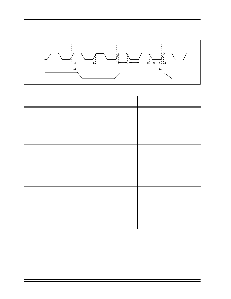
FIGURE 23-6:
EXTERNAL CLOCK TIMING (ALL MODES EXCEPT PLL)
TABLE 23-6:
EXTERNAL CLOCK TIMING REQUIREMENTS
Param.
No.
Symbol
Characteristic
Min
Max
Units
Conditions
1A
FOSC
External CLKI Frequency(1)
DC
1
MHz
XT, RC Oscillator modes
DC
40
MHz
EC Oscillator mode
DC
31.25
kHz
LP Oscillator mode
Oscillator Frequency(1)
DC
4
MHz
RC Oscillator mode
0.1
4
MHz
XT Oscillator mode
4
20
MHz
HS Oscillator mode
5
200
kHz
LP Oscillator mode
1TOSC
External CLKI Period(1)
1000
—
ns
XT, RC Oscillator modes
50
—
ns
HS Oscillator mode
25
—
ns
EC Oscillator mode
Oscillator Period(1)
250
—
ns
RC Oscillator mode
250
1
s
XT Oscillator mode
50
250
ns
HS Oscillator mode
100
250
ns
HS +PLL Oscillator mode
5200
s
LP Oscillator mode
2TCY
Instruction Cycle Time(1)
100
—
ns
TCY = 4/FOSC, Industrial
160
—
ns
TCY = 4/FOSC, Extended
3TOSL,
TOSH
External Clock in (OSC1)
High or Low Time
30
—
ns
XT Oscillator mode
2.5
—
s
LP Oscillator mode
10
—
ns
HS Oscillator mode
4TOSR,
TOSF
External Clock in (OSC1)
Rise or Fall Time
—
20
ns
XT Oscillator mode
—
50
ns
LP Oscillator mode
—
7.5
ns
HS Oscillator mode
Note 1:
Instruction cycle period (TCY) equals four times the input oscillator time base period for all configurations
except PLL. All specified values are based on characterization data for that particular oscillator type under
standard operating conditions with the device executing code. Exceeding these specified limits may result
in an unstable oscillator operation and/or higher than expected current consumption. All devices are tested
to operate at “min.” values with an external clock applied to the OSC1/CLKI pin. When an external clock
input is used, the “max.” cycle time limit is “DC” (no clock) for all devices.
OSC1
CLKO
Q4
Q1
Q2
Q3
Q4
Q1
1
2
33
4
发布紧急采购,3分钟左右您将得到回复。
相关PDF资料
PIC18F1330T-I/ML
IC PIC MCU FLASH 4KX16 28QFN
PIC18F65J50T-I/PT
IC PIC MCU FLASH 16KX16 64TQFP
PIC18F83J11T-I/PT
IC PIC MCU FLASH 4KX16 80TQFP
PIC16LF627-04/P
IC MCU FLASH 1KX14 COMP 18DIP
PIC18F86J55T-I/PT
IC PIC MCU FLASH 48KX16 80TQFP
PIC18F43K22-I/MV
MCU PIC 8KB FLASH 40QFN
PIC16C55A-04I/P
IC MCU OTP 512X12 28DIP
PIC18LF43K22-I/MV
MCU PIC 8KB FLASH 40UQFN
相关代理商/技术参数
PIC18F1230T-I/SS
功能描述:8位微控制器 -MCU 4KB Flash 256 RAM RoHS:否 制造商:Silicon Labs 核心:8051 处理器系列:C8051F39x 数据总线宽度:8 bit 最大时钟频率:50 MHz 程序存储器大小:16 KB 数据 RAM 大小:1 KB 片上 ADC:Yes 工作电源电压:1.8 V to 3.6 V 工作温度范围:- 40 C to + 105 C 封装 / 箱体:QFN-20 安装风格:SMD/SMT
PIC18F1320-E/ML
功能描述:8位微控制器 -MCU 8KB 256 RAM 16 I/O RoHS:否 制造商:Silicon Labs 核心:8051 处理器系列:C8051F39x 数据总线宽度:8 bit 最大时钟频率:50 MHz 程序存储器大小:16 KB 数据 RAM 大小:1 KB 片上 ADC:Yes 工作电源电压:1.8 V to 3.6 V 工作温度范围:- 40 C to + 105 C 封装 / 箱体:QFN-20 安装风格:SMD/SMT
PIC18F1320-E/P
功能描述:8位微控制器 -MCU 8KB 256 RAM 16 I/O RoHS:否 制造商:Silicon Labs 核心:8051 处理器系列:C8051F39x 数据总线宽度:8 bit 最大时钟频率:50 MHz 程序存储器大小:16 KB 数据 RAM 大小:1 KB 片上 ADC:Yes 工作电源电压:1.8 V to 3.6 V 工作温度范围:- 40 C to + 105 C 封装 / 箱体:QFN-20 安装风格:SMD/SMT
PIC18F1320-E/SO
功能描述:8位微控制器 -MCU 8KB 256 RAM 16 I/O RoHS:否 制造商:Silicon Labs 核心:8051 处理器系列:C8051F39x 数据总线宽度:8 bit 最大时钟频率:50 MHz 程序存储器大小:16 KB 数据 RAM 大小:1 KB 片上 ADC:Yes 工作电源电压:1.8 V to 3.6 V 工作温度范围:- 40 C to + 105 C 封装 / 箱体:QFN-20 安装风格:SMD/SMT
PIC18F1320-E/SS
功能描述:8位微控制器 -MCU 8KB 256 RAM 16 I/O RoHS:否 制造商:Silicon Labs 核心:8051 处理器系列:C8051F39x 数据总线宽度:8 bit 最大时钟频率:50 MHz 程序存储器大小:16 KB 数据 RAM 大小:1 KB 片上 ADC:Yes 工作电源电压:1.8 V to 3.6 V 工作温度范围:- 40 C to + 105 C 封装 / 箱体:QFN-20 安装风格:SMD/SMT
PIC18F1320-H/ML
功能描述:8位微控制器 -MCU 8KB FL 256RAM 16 I/O RoHS:否 制造商:Silicon Labs 核心:8051 处理器系列:C8051F39x 数据总线宽度:8 bit 最大时钟频率:50 MHz 程序存储器大小:16 KB 数据 RAM 大小:1 KB 片上 ADC:Yes 工作电源电压:1.8 V to 3.6 V 工作温度范围:- 40 C to + 105 C 封装 / 箱体:QFN-20 安装风格:SMD/SMT
PIC18F1320-H/P
功能描述:8位微控制器 -MCU 8KB FL 256RAM 16 I/O RoHS:否 制造商:Silicon Labs 核心:8051 处理器系列:C8051F39x 数据总线宽度:8 bit 最大时钟频率:50 MHz 程序存储器大小:16 KB 数据 RAM 大小:1 KB 片上 ADC:Yes 工作电源电压:1.8 V to 3.6 V 工作温度范围:- 40 C to + 105 C 封装 / 箱体:QFN-20 安装风格:SMD/SMT
PIC18F1320-H/SO
功能描述:8位微控制器 -MCU 8KB FL 256RAM 16 I/O RoHS:否 制造商:Silicon Labs 核心:8051 处理器系列:C8051F39x 数据总线宽度:8 bit 最大时钟频率:50 MHz 程序存储器大小:16 KB 数据 RAM 大小:1 KB 片上 ADC:Yes 工作电源电压:1.8 V to 3.6 V 工作温度范围:- 40 C to + 105 C 封装 / 箱体:QFN-20 安装风格:SMD/SMT